Google Frozen v2 Chip Bakes Gemini Into Silicon for Up to 10x Efficiency
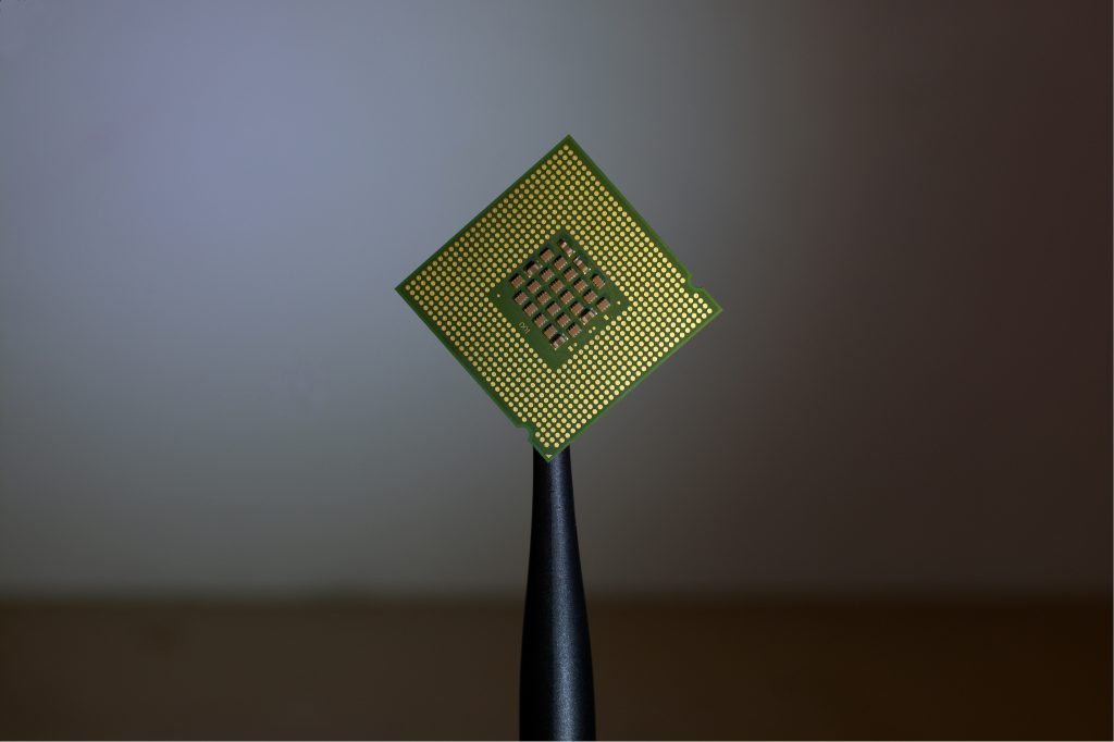
Google’s Frozen v2 chip is the most talked-about piece of silicon in the AI world this week, after a report revealed the company is etching part of its Gemini model architecture directly into hardware. First detailed by Tom’s Hardware, based on reporting from The Information, the project points to a future where an AI model and the chip that runs it are designed as a single, inseparable unit.
What the Frozen v2 Chip Actually Does
A conventional accelerator like Google’s Tensor Processing Unit (TPU) is built to run many different AI models. The Frozen v2 chip flips that logic. Instead of staying flexible, it freezes many of the architectural decisions behind Gemini — the layer structure, the attention patterns, the data pathways — into the transistors themselves. By hardwiring those choices, the design reduces the number of steps it takes per query and cuts the amount of data it has to shuttle back and forth. The result, according to engineers on the project, is silicon that could serve six to ten times more tokens per watt than Google’s newest TPUs during inference.
Why Hardwiring Gemini Changes the Math
Inference — the work of actually answering a user’s prompt — now dominates AI’s energy bill. Every Gemini query in Search, Workspace, and the Gemini app draws power, and at Google’s scale even small efficiency gains translate into enormous savings. Six-to-ten-times more tokens per watt is not a minor tweak; it is the kind of leap that could reshape the economics of running frontier models. That is why investors reacted quickly, nudging Alphabet’s stock higher on the report even though Google has not officially confirmed the project.
- Efficiency: 6–10x more tokens per watt than current TPUs, measured on inference only.
- Timeline: deployment targeted for as soon as 2028.
- Scope: a limited run, not a full TPU replacement.
A Trial Run, Not a TPU Replacement
Google does not plan to build the Frozen v2 chip at TPU volumes. Sources describe it as a trial run for more specialized silicon that Google might pursue once model designs stop changing so quickly. It would sit alongside the eighth-generation TPU line unveiled at Cloud Next in April, which already split into separate training and inference variants. In other words, this is a bet on a specific idea: that at some point, the shape of a model is worth locking into hardware.
The Risk of Freezing a Model in Silicon
That bet carries obvious danger. AI architectures have changed dramatically year over year, and hardware that hardwires today’s Gemini could become expensive dead weight if next year’s breakthrough demands a different design. Chips take years and billions of dollars to bring to production, so timing is everything. Google appears to be hedging by keeping the project small and treating 2028 as a proving ground rather than a mass-market launch. If it works, the Frozen v2 chip could mark the start of a new phase in AI hardware — one where the model and the metal are co-designed from the ground up.
The Bottom Line
Custom AI silicon is no longer just about faster matrix math; it is about squeezing every last token out of each watt. Google’s Frozen v2 chip is the clearest signal yet that the industry’s next efficiency war will be fought at the level of architecture itself. Whether hardwiring Gemini proves visionary or premature, it shows how far hyperscalers will go to control the cost of inference.
Related on DAILYSIM: Gemini 3.5 Delay Wipes $200 Billion Off Alphabet as Coding Falls Short and AMD Helios Ships as Microsoft Becomes the First Hyperscaler to Deploy It at Scale.