Sub-1nm Chip Breakthrough: IBM Unveils a 0.7nm Nanostack With 100 Billion Transistors
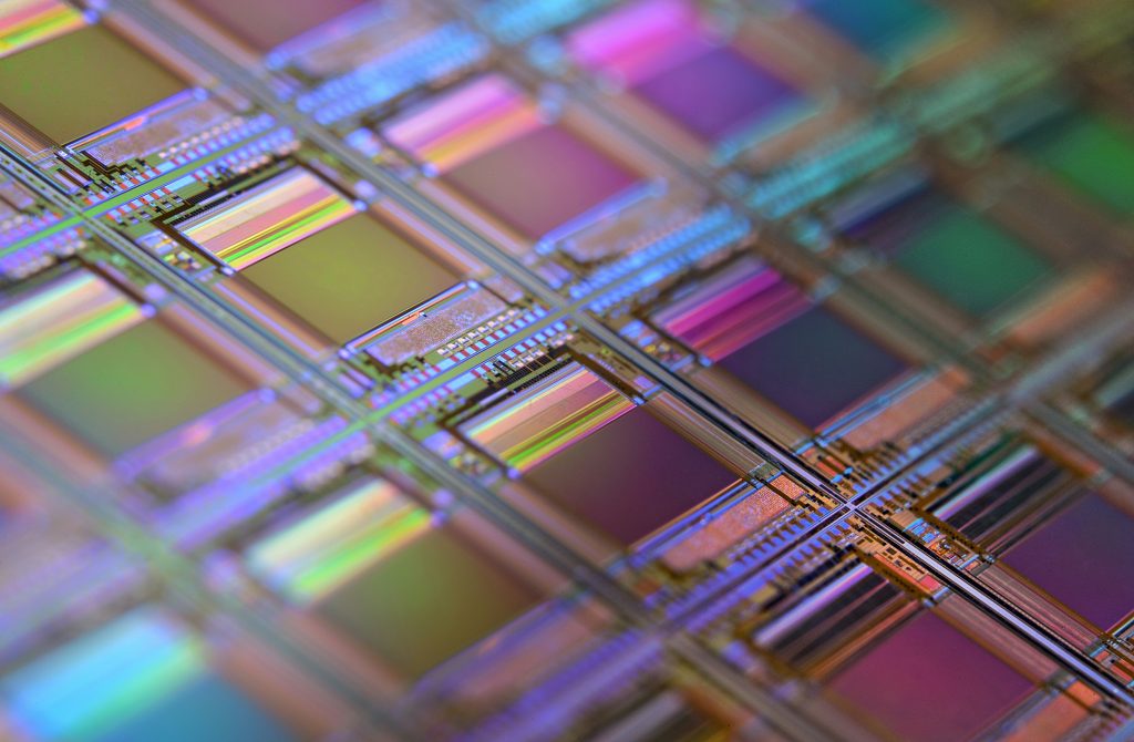
IBM has just crossed one of computing’s most stubborn barriers with the world’s first sub-1nm chip — a 0.7-nanometer test device that crams nearly 100 billion transistors onto a sliver of silicon the size of a fingernail. It is the first time logic technology has ever reached below the 1nm node, and it lands right as the AI industry is starving for faster, cooler silicon.
For an industry that has spent years worrying that Moore’s Law was finally running out of road, the sub-1nm chip is a jolt of optimism. It does not just shrink transistors a little further; it changes how they are built.
Inside IBM’s sub-1nm chip and the ‘nanostack’
Rather than keep squeezing transistors across a flat, two-dimensional plane, IBM stacks and staggers them vertically in 3D layers — an approach it calls ‘nanostack.’ Using a technique known as 3D sequential integration, the company built logic at a 0.7nm (7 angstrom) node, packing close to 100 billion transistors into fingernail-sized silicon. That is nearly double the density of the 2nm nanosheet chip IBM revealed back in 2021.
The shift to vertical stacking is the key idea. Once you can no longer make features meaningfully smaller, you build upward instead — and the nanostack approach also delivers a 40% improvement in SRAM scaling, a notoriously hard part of any process node to shrink.
Why a sub-1nm chip matters for AI
The timing is not an accident. Every frontier AI model is bottlenecked by the cost, power, and memory bandwidth of the hardware it runs on. A denser, more efficient sub-1nm chip directly attacks all three. IBM says the new design delivers up to 50% higher performance, or 70% greater energy efficiency, compared with its 2nm predecessor — exactly the kind of leap that data-center operators drowning in electricity bills want to hear.
- Density: ~100 billion transistors on a fingernail-sized die.
- Performance: up to 50% faster than 2nm at the same power.
- Efficiency: up to 70% lower energy at the same performance.
- Memory: 40% SRAM scaling to feed high-bandwidth AI workloads.
How the sub-1nm chip stacks up against 2nm
IBM’s 2nm process is only now ramping into commercial production with manufacturing partners, so the 0.7nm result is best read as a research milestone that proves the roadmap is still open. According to IBM’s own announcement, the breakthrough extends the runway for semiconductor scaling by at least another decade. MIT Technology Review framed it as evidence that Moore’s Law, long pronounced dead, may have a few more nodes left in it.
What it means for TSMC and Samsung
IBM no longer manufactures chips at scale itself; it licenses and co-develops process technology with partners. That makes the nanostack result a shot across the bow for foundry leaders TSMC and Samsung, both racing toward their own angstrom-era nodes. Whoever turns 3D-stacked transistors into a manufacturable, high-yield process first will hold enormous leverage over the companies building the world’s AI infrastructure — from Nvidia to the hyperscalers now designing their own silicon.
When can you actually buy one?
Not soon. IBM is targeting production within roughly five years and has not said how it will commercialize the nanostack architecture. For now, the company’s near-term focus stays on helping foundry partners scale today’s 2nm technology. The sub-1nm chip is a demonstration that the path forward exists — not a product you can order this year.
The bottom line
A working sub-1nm chip reframes the whole ‘end of Moore’s Law’ debate. By going vertical with nanostack, IBM has shown there is at least a decade of scaling left — and that the next era of AI hardware may be defined less by how small transistors get and more by how cleverly they are stacked.
Related on DAILYSIM: OpenAI’s Jalapeno inference chip and Google’s Gemini compute crunch.